RF circuits, designed right.
RF Next Design is an independent RF design practice: low noise amplifiers, power amplifiers, RF switches and mixed-signal PCBs, plus hands-on design consultation.
Drag to rotate
The best RF products are won in the schematic and the stack-up.
Simulate first Matching, stability, noise and linearity are worked out in simulation before any board is built.
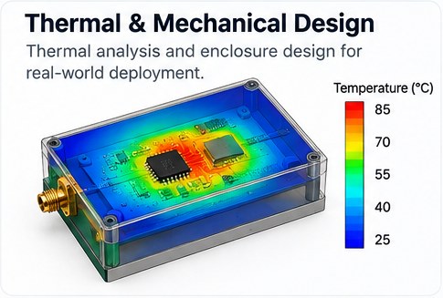
Layout with care Grounding, stack-up, isolation and thermal paths decide whether the simulation survives on the PCB.
Measure everything VNA, spectrum analyzer and noise measurements confirm the circuit meets its target.
What we design.
Five core services, from a single amplifier stage to a complete mixed-signal board.
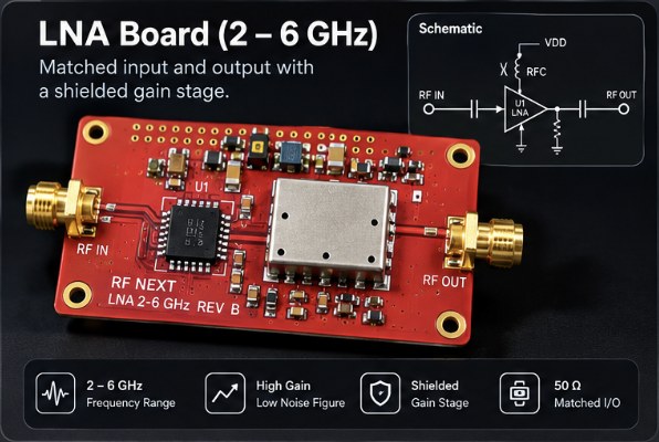
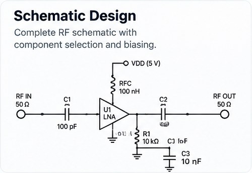
Low noise amplifiers MMIC and discrete pHEMT LNAs tuned for noise figure, gain and stability.
Impedance and noise matching Stability across the band Fabrication on Rogers substrate Power amplifiers 10–25 W GaN amplifier stages with attention to linearity, efficiency and heat.
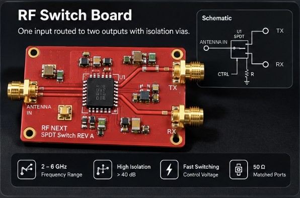
Class selection and biasing ACPR and IP3 optimisation Thermal and supply design RF switches Switch networks for transmit and receive paths, with a focus on isolation and insertion loss.
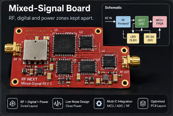
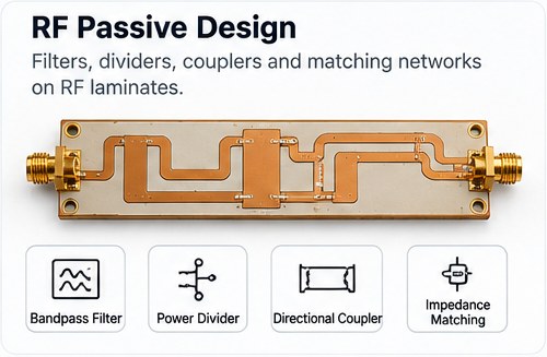
Part selection and trade-offs Control and driver circuits Layout for isolation Mixed-signal PCB RF, analog, digital and power on one board without them interfering.
2–8 layer stack-ups Altium Designer and KiCad BOM and component selection Design consultation Independent advice on architecture, parts and risks, from first idea to prototype review.
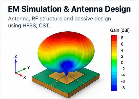
Architecture and block diagrams Design reviews before a PCB spin Debug and measurement help Simulation and test Circuit and EM simulation, then VNA and spectrum validation on the bench.
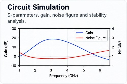
S-parameters, noise, stability EVM, harmonics, linearity Documentation and reports
Results from recent designs.
Measured and simulated targets from amplifier and front-end work.
<1.2 dB pHEMT LNA noise figure Custom discrete LNA with matched noise and gain, fabricated and tested.
2–6 GHz MMIC LNA High gain and stability across the band, with impedance and noise optimisation.
10–25 W GaN power amplifier High-power stages for wideband radio transmit chains.
DC–10 GHz Amplifier simulation Circuit and EM design from DC to 10 GHz.
Boards we lay out.
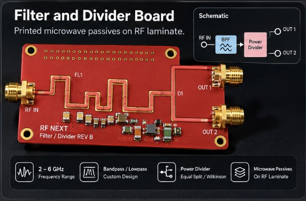
Real RF board designs with their schematics and key specifications.
From schematic to prototype.
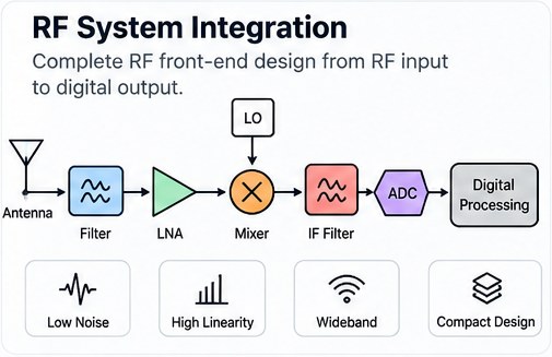
Every stage of an RF design, from the first schematic to thermal checks.
Inside the modules.
Drag up on a module to open it and see what is inside. Drag down to close it.
Drag up to open, down to close Open the module
Amplifier module Enclosure, PCB, heatsink and two SMA connectors.
Drag up to open, down to close Open the module
RF switch module Enclosure, PCB, RF shield and three SMA ports: antenna, TX and RX.
Drag to rotate
Space and wireless communication.
Radio links over a few kilometres or 36,000 km follow the same maths. We plan them before hardware is built.
Satellite links Link budgets for GEO and other orbits, including path loss, antenna gain and margin.
Point-to-point and multipoint Terrestrial links planned for range, throughput and reliability.
Frequency planning Channel selection and interference mitigation before deployment.
Coverage and propagation Terrain-aware coverage estimates and optimisation.
Consultation, step by step.
Bring a specification or a half-working prototype. We work through it in the same order every time.
Specification Frequency, gain, noise, power, size and cost targets. Architecture and parts Block diagram and component trade-offs. Simulation Matching, stability and linearity in simulation. Schematic and layout Stack-up, RF routing, grounding and BOM. Prototype and measurement VNA, spectrum and noise checks against target.